K. Eriguchi et al., DOI: 10.5772/36394
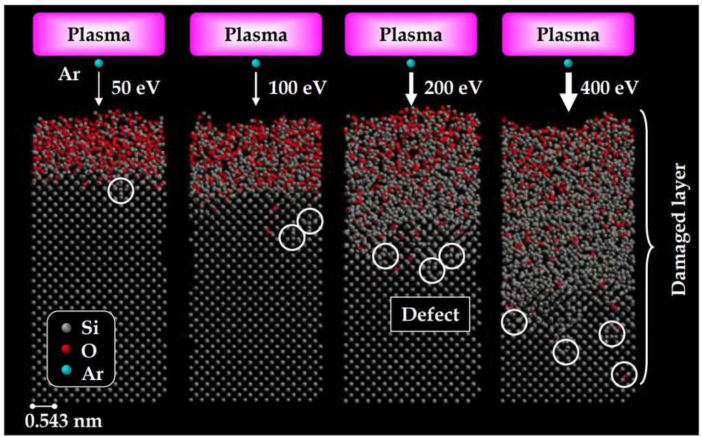
Etching is a key step in semiconductor process. Up to date, most of etching process had been conducted by using plasma, generating highly energetic radicals in order to make a volatile etch species by the reaction with materials. However, damage induced by the energetic species cannot be negligible anymore as device scales down to sub-10 nm. Thus, a need of a new etching process which doesn’t use plasma or high energy radicals becomes more and more important.
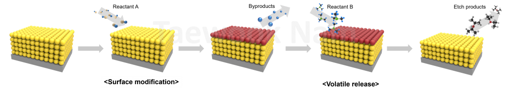
Fig. Schematic of atomic layer etching (ALE)
Thermal atomic layer etching (ALE), the opposite reaction of atomic layer deposition (ALD), is considered as a promising etch technique that can overcome the damage. ALE is based on sequential, self-limiting surface reaction, same with ALD. As shown in the figure above, a precursor (or reactant A) modifies surface of a material, then a following precursor reacts with the modified layer, making volatile species. In this manner, the ALE ensures 1) atomic thickness controllability, 2) large area uniformity, and 3) isotropic etching. In particular, the traditional etching techniques such as reactive ion etching (RIE) have anisotropic etching due to the directionality of energetic ion species, whereas thermal ALE etches isotropically, it can be used for uniform etching to fabricate 3-d structured devices such as nanowire field effect transistor (NW FET).
Copyrightⓒ 2018-2024. Taewook Nam. All right reserved.